Manufacturing Process
Manufacturing Process Flow
Product information
We provide integrated, end-to-end production from single crystal growth through mirror-finish polishing. In the single crystal pulling process, we grow the single crystal and perform cutting and cylindrical grinding. In the CW manufacturing process, the single crystal ingot is sliced into wafers, and surface flatness is improves by lapping and chemical etching. In the PW manufacturing process, multi stage polishing achieves a mirror finish surface. For special requirement, we can provide back-side damage and other custom processing to meet customer specifications.
| Single Crystal Pulling process | Detailed single crystal pulling process |
|---|---|
| Etched wafer manufacturing process (Called CW manufacturing process) |
Etched wafer processing details |
| Polished wafer manufacturing process (Called PW manufacturing process) |
Polished wafer processing details |
| Inspection process | inspection processing details |
Special customize
We also accept Backside damage, Thermal oxidation (SiO2 film), and Laser marking of silicon wafers.
Inspection
We guarantee the quality of our products through inspection.
Single Crystal
Single Crystal Pulling process
We perform single crystal growth, cutting, and cylindrical grinding.
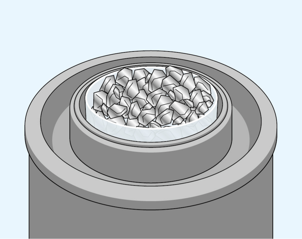
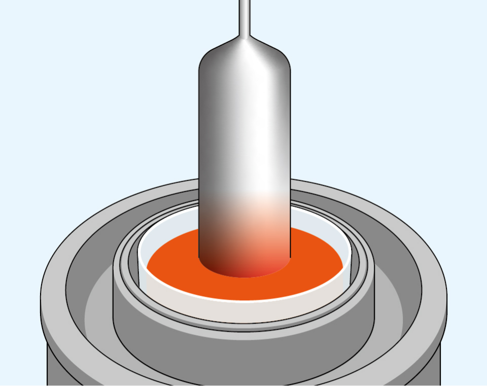
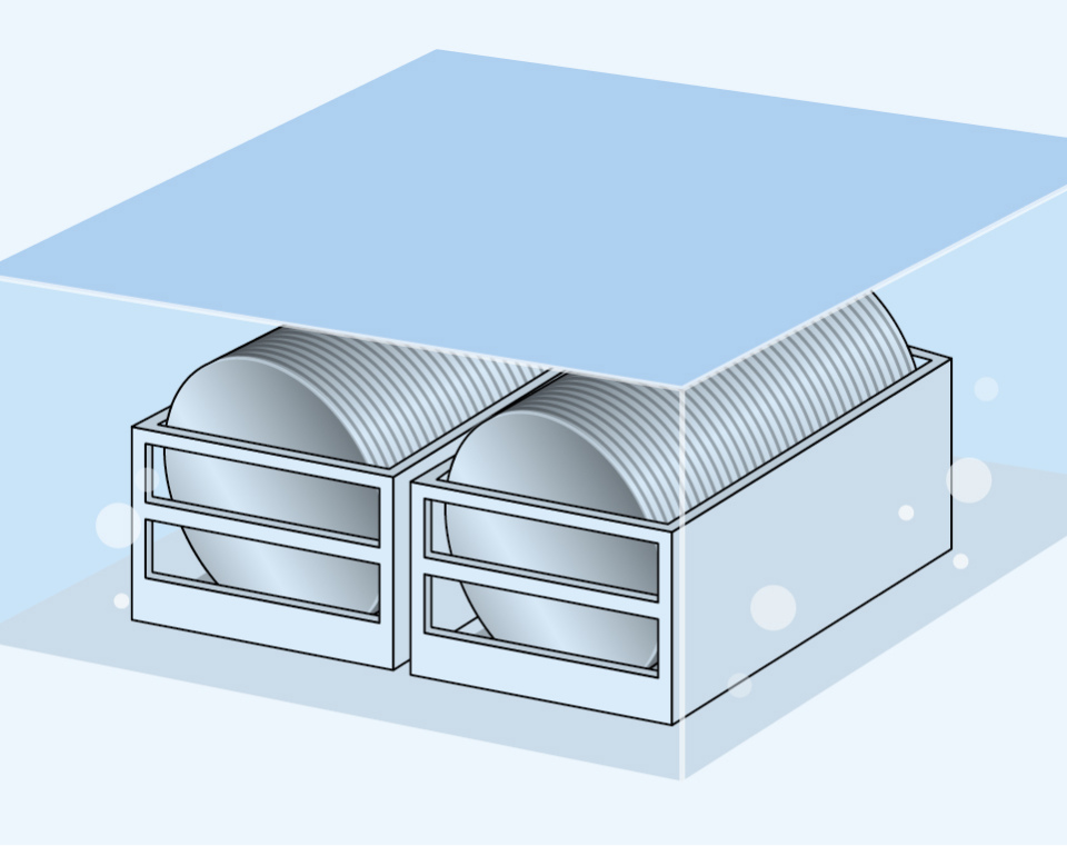
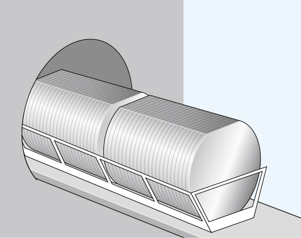
Crystal growth by the Czochralski method: polysilicon feedstock and dopant are melted in a quartz crucible at the temperatures near the melting point,and a single crystal is grown with an orientation defined by the seed crystal.
Cutting and Cylindrical Grinding Process
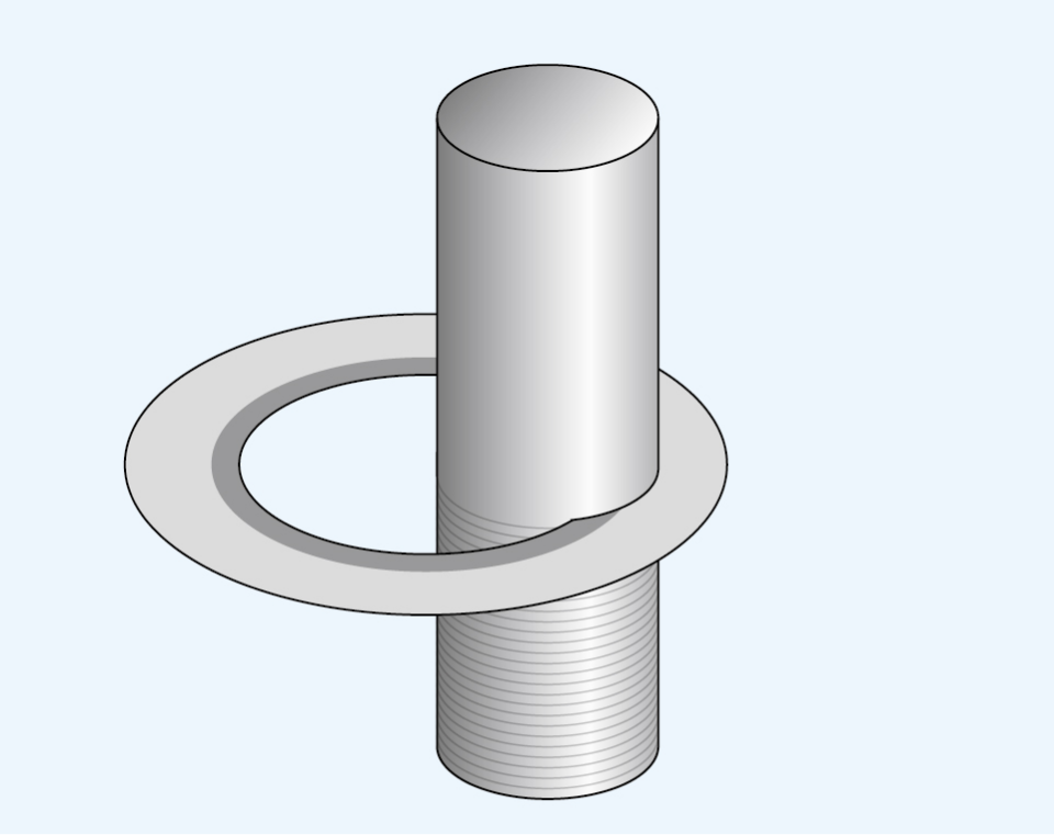
We cut the single crystal into the blocks and perform cylindrical grinding to achieve a specified diameter. Orientation Flat and Notch are machined to identify the crystallographic orientation. Additional process can be provided upon request.
Crystal inspection
Using test wafers, we inspect crystal defects, resistivity, and other quality parameters.
Etched wafer
Etched wafer manufacturing process
From Slicing through etching, the ingot is sawn into wafer form, followed by edge shaping, surface lapping, and removal surface damage. And oxygen-related donors are annihilated through annealing.
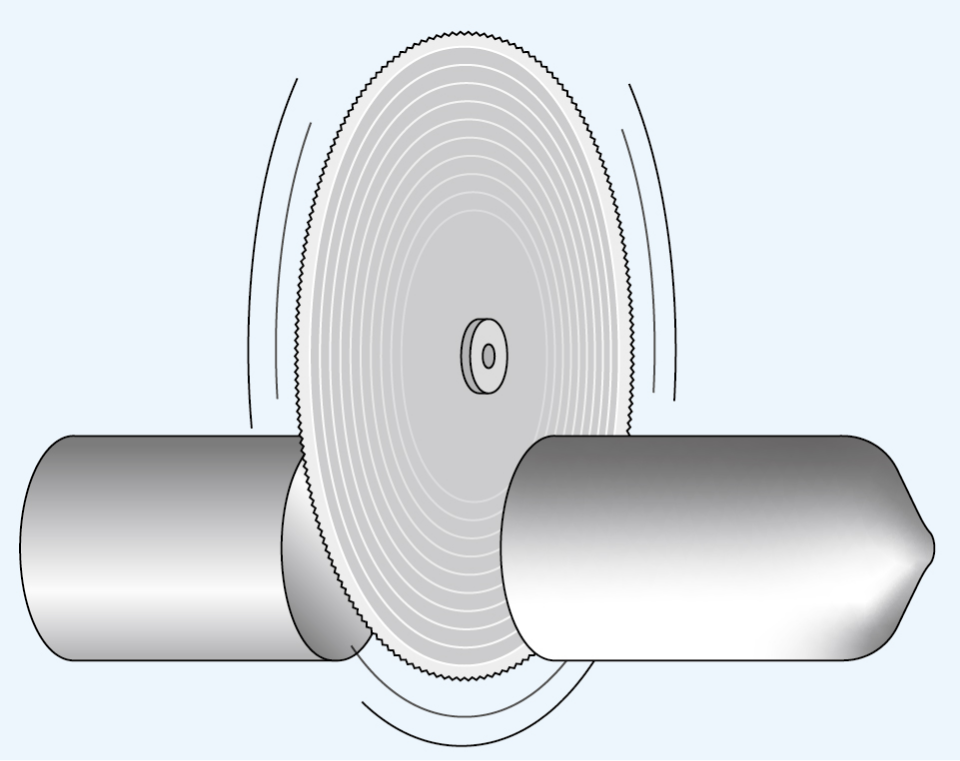
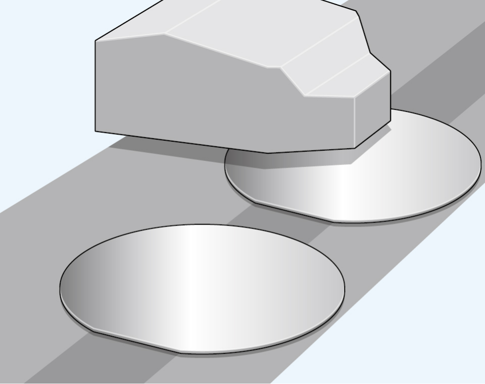
Slicing
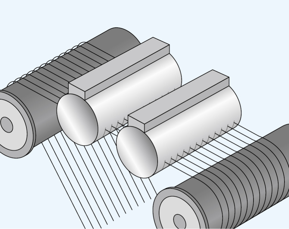
Ingots will be cut into wafer shape using wire saw and inner diameter saw.
Beveling
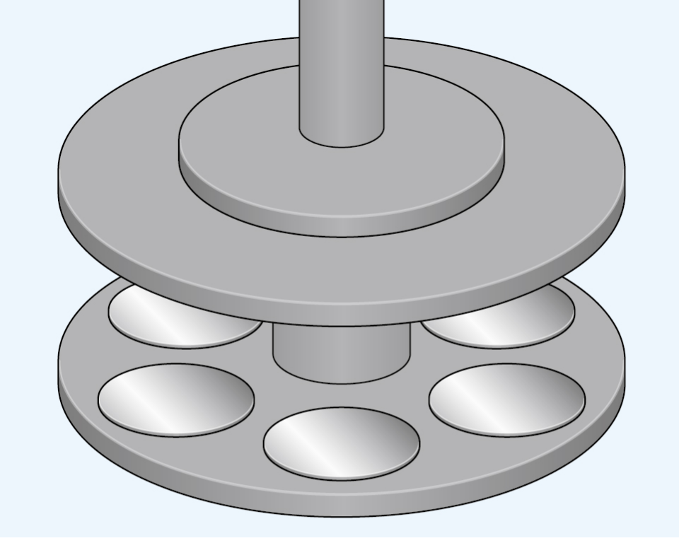
To prevent chipping and particle generation, we perform edge beveling of the wafer perimeter. This process also a uniform wafer diameter.
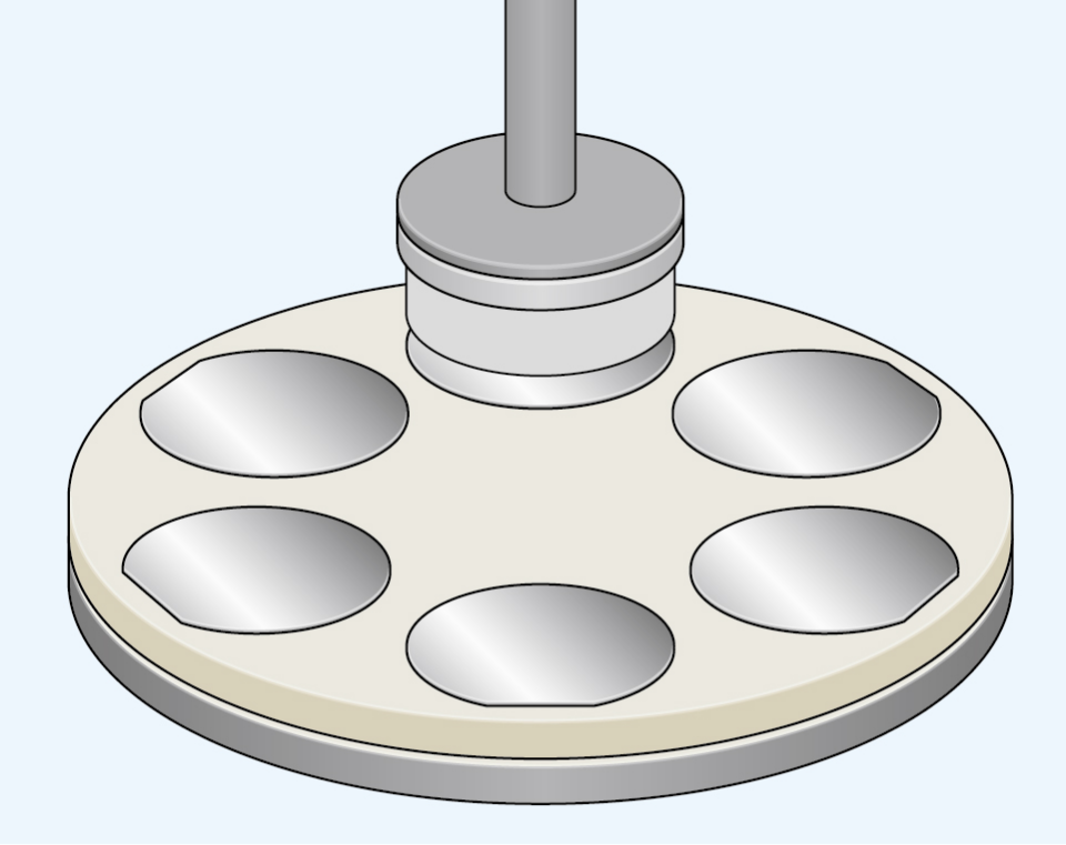
Lapping
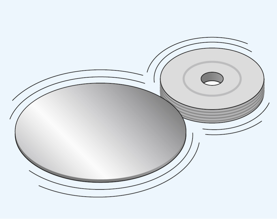
We use surface lapping to control wafer thickness and flatness.
Etching
Using wet chemical etching, we remove the surface damage layer from the preceding steps.
Annihilation
To recover the original resistivity,
oxygen-related donors are annihilated through annealing.
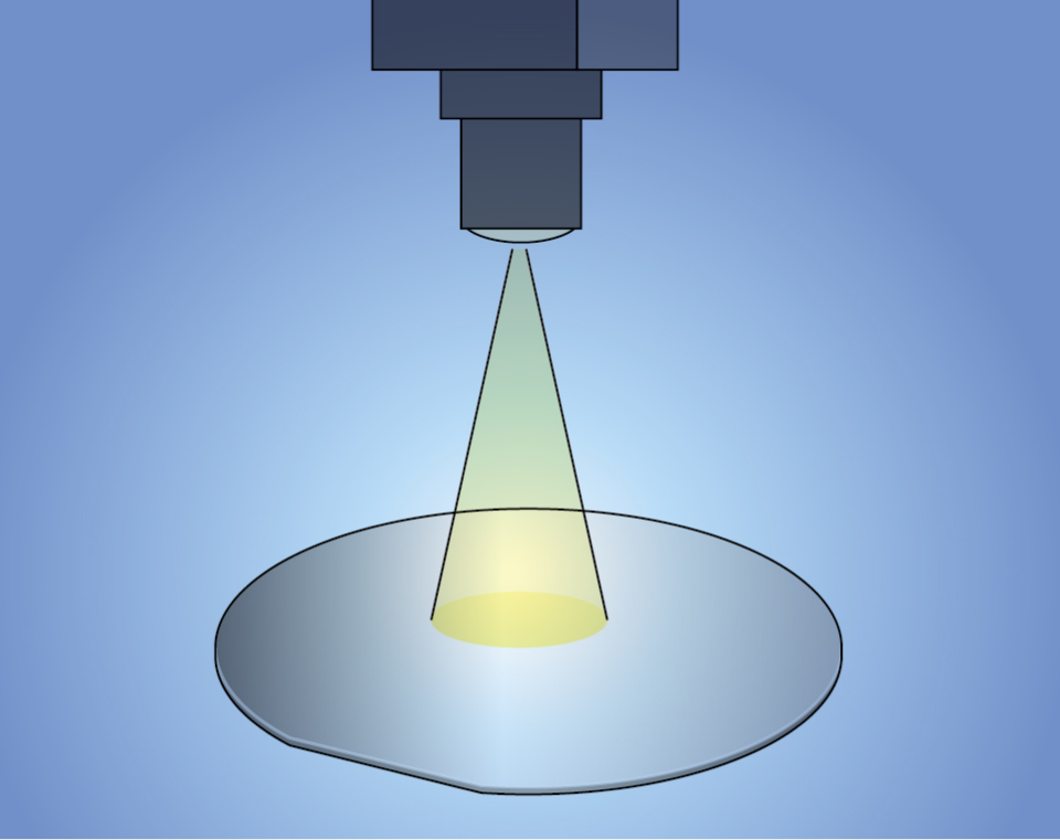
In-Process inspection
Product quality is assured through inspection.
We conduct visual surface inspection, flatness measurements using specialized equipment, and tests of electrical characteristics.
Polished wafer
Plate bonding
The wafer is bonded to ceramics plate to enable mirror polishing wafer surface.
Mirror polishing
Chemical mechanical polishing yields a highly flatness, low-contamination mirror finish.
Final inspection
After cleaning to improve wafer cleanliness, product quality is assured through final inspection.
We conduct visual surface inspection, flatness measurements using specialized equipment, and tests of electrical characteristics.