Magneto-optical device
Applications: Magneto-optical device
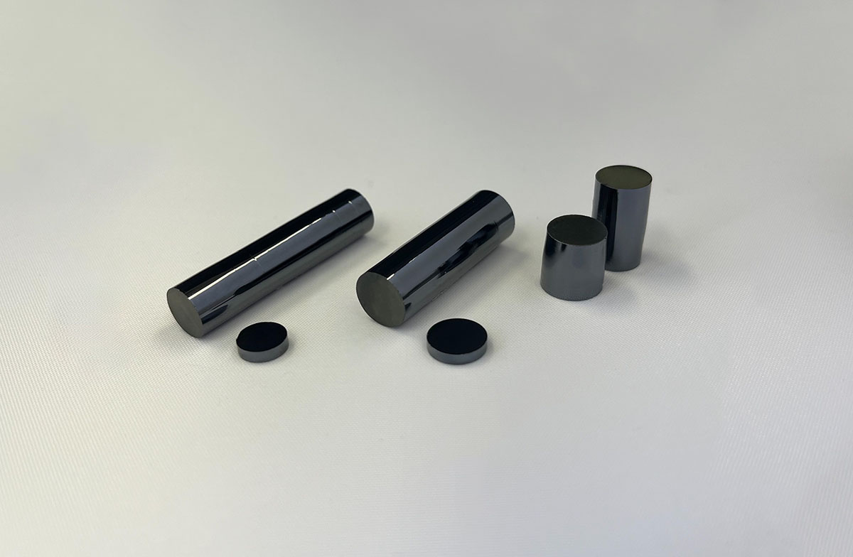
YIG (Yttrium Iron Garnet)
Product information
YIG (Yttrium Iron Garnet) is a garnet-type ferrite crystal with magneto-optical properties. Using a proprietary manufacturing process based on the Floating Zone method, we produce high-purity single crystal. These high purity YIG single crystal are used in components for telecommunications equipment, such as optical isolators and magnetic-resonance filters. We can also offer customized substitutional rare-earth Iron garnet for various magneto-optical device. Please feel me to contact us to discuss your requirement.
Custom specifications available upon request. Please feel free to contact us.
For Semiconductor
Applications: Substrate for GaN (Gallium Nitride) epitaxial growth.
ST Wafer
Product information
ST wafer is improved mechanical strength by heavily B and Ge codoping. It exhibits heat resistance to thermal stress during high-temperature processing, suppressing slip and warpage. It is ideally suited as a substrate for Hetero-epitaxial growth such as GaN which has been attracting increasing attention in recent years.
Applications: Substrate for the MEMS
Ultra High Flatness Wafer
Product information
We provide high flatness 4 inch and 6 inch wafers for MEMS and filter applications.
TTV≦3 um, with controllable geometry and taper, enable uniform device layers in composite wafers. Geometry specifications are guaranteed up to a 1 mm edge exclusion, and ESFQR guarantees are ails available. We can accommodate non-SEMI / JEITA thickness, helping to simplify your device process.
Applications: For photonics and photonic integrated circuits
Thick Film Wafer
Product information
We supply thick thermal oxide wafers with oxide thickness up to 15 um.
They feature excellent thickness uniformity and a stable refractive index, making them suitable for optical and highly insulating dielectric layers.
The specification of the silicon wafers used for oxide growth can also be customized.
Material for far infrared rays
HT Silicon
Product information
HT Silicon is under development silicon material, which improved less transmittance of 9um needs for human detection at far-infrared regions. Since this silicon material is low cost comparing with other materials for far-infrared transmitted materials such as Germanium, HT silicon is suitable material for low cost and mass production performance in lens of night vision camera of car or infrared camera.
Silicon Single Crystal by the Optical Floating Zone method.
Product information
Coming soon...
Polycrystalline germanium
Product information
We recover scraps (end materials, cutting chips) as low purity germanium, purifies to over 5N(99.999%) high purified polycrystalline germanium. This high purified polycrystalline germanium is utilized as alloys, target materials, and reposition source materials.
Contract Service for Crystal Growth
We would like respond to your requests at a higher level with our own crystal growth techniques and products.
- Crystal growth service (Floating Zone method)
- Contract Service for Crystal Growth
- If you have any questions
Please feel free to contact Us