For semiconductor
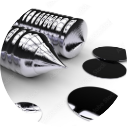
Silicon Wafer
Product information
We manufacture and supply semiconductor-grade silicon single crystals and wafers, operating an end-to-end production system from crystal growth and mirror polished wafer fabrication. By cultivating the base crystals in-house, we are able to provide solutions tailored to each customer's specifications.
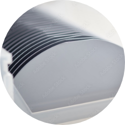
1.Silicon Single Crystal
Specification
- Method; CZ method, FZ method
- Diameter: 4, 5, 6, (8) inch
- Dopant; B, P, Sb, (As)
- Orientation: <100>, <111>, <110>
- Resistivity: 0.001 ~ 40.0 Ohm・cm
- Oxygen Concentration: 10 ~ 18×1017 atoms/cm3 (ASTM FM121-79)
- Carbon Concentration: ≤5×10¹⁶ atoms/cm3
- OISF:≤50 pcs/cm2
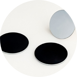
2.Wafer Lineup
-
Polished Wafer
Mirror polished wafer with low surface roughness, high flatness, and ultra-clean surfaces.
-
Etched Wafer
Wafer with the removal subsurface damage.
-
Lapped Wafer
Wafer with the improvement of the flatness and suppressed subsurface damage.
Custom specifications available upon request. Please feel free to contact us
3.Optional Specification
We also accept Backside damage, Thermal oxidation (SiO2 film), and Laser marking of silicon wafers.